-- by Weijun Zhang

If we hear, we forget; if we see, we remember; if we do, we understand.
-- Proverb
Table of Contents
 Foreword Foreword |
| Basic Logic GatesCombinational Logic DesignTypical Combinatinal Logic Components | Latch and Flip-FlopsSequential Logic DesignTypical Sequential Logic Components |
| Custom Single-Purpose Processor DesignGeneral-Purpose Processor Design Appendix: Modeling an industry core |
<> HDL (Hardware Description Language) based design has established itself as the modern approach to design of digital systems, with VHDL (VHSIC Hardware Description Language) and Verilog HDL being the two dominant HDLs. Numerous universities thus introduce their students to VHDL (or Verilog). The problem is that VHDL is complex due to its generality. Introducing students to the language first, and then showing them how to design digital systems with the language, tends to confuse students. The language issues tend to distract them from the understanding of digital components. And the synthesis subset issues of the language add to the confusion.
Foreword (by Frank Vahid)
We developed the following tutorial based on the philosophy that the beginning student need not understand the details of VHDL -- instead, they should be able to modify examples to build the desired basic circuits. Thus, they learn the importance of HDL-based digital design, without having to learn the complexities of HDLs. Those complexities can be reserved for a second, more advanced course. The examples are mostly from the textbook Embedded System Design by Frank Vahid and Tony Givargis. They start from basic gates and work their way up to a simple microprocessor. Most of the examples have been simulated by Aldec ActiveHDL Simulator and Synopsys Design Analyzer, as well as synthesized with Synopsys Design Compiler . Several sequential design examples have been successfully tested onXilinx Foundation Software and FPGA/CPLD board.

Basic Logic Gates
(ESD Chapter 2: Figure 2.3)
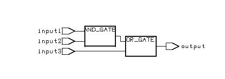
Every VHDL design description consists of at least one entity / architecture pair, or one entity with multiple architectures. The entity section of the HDL design is used to declare the I/O ports of the circuit, while the description code resides within architecture portion. Standardized design libraries are typically used and are included prior to the entity declaration. This is accomplished by including the code "library ieee;" and "use ieee.std_logic_1164.all;".
Combinational Logic Design
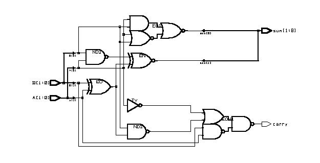
(ESD Chapter 2: Figure 2.4)
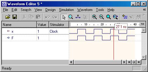
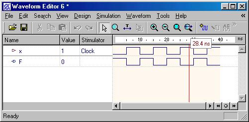
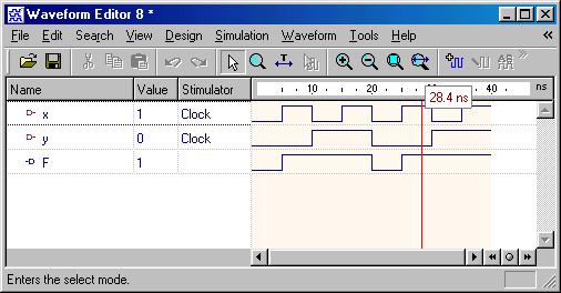
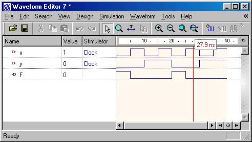
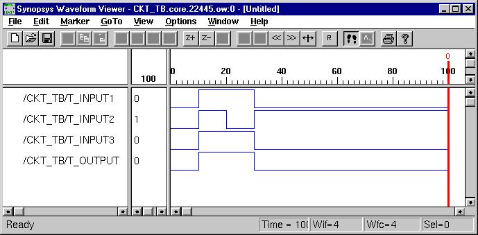
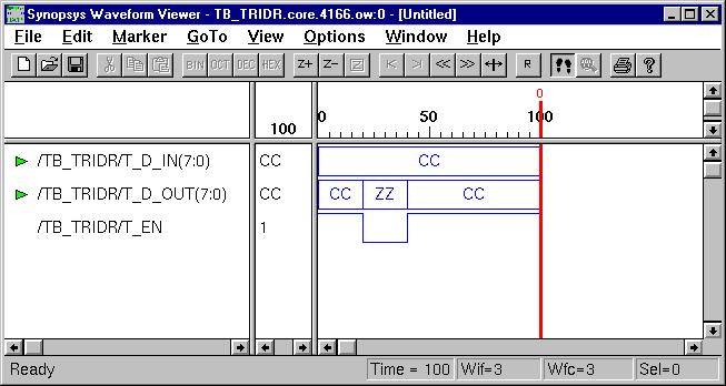
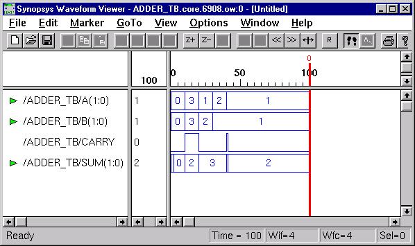
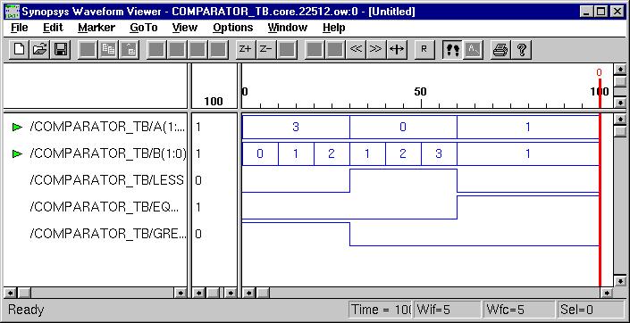
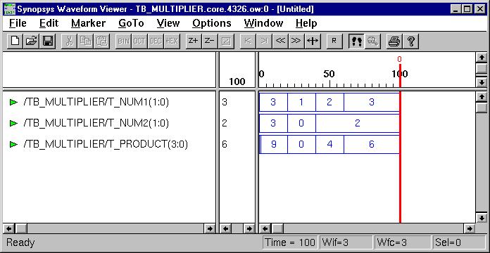
We use port map statement to achieve the structural model (components instantiations). The following example shows how to write the program to incorporate multiple components in the design of a more complex circuit. In order to simulate the design, a simple test bench code must be written to apply a sequence of inputs (Stimulators) to the circuit being tested (UUT). The output of the test bench and UUT interaction can be observed in the simulation waveform window.
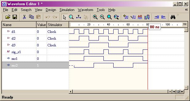
Discussion I: Signal vs. Variable: Siganls are used to connect the design components and must carry the information between current statements of the design. On the other hand, variables are used within process to compute certain values. The following example shows their difference:
Signal/Variable Example
Behavior Code
Behavior Simulation
Typical Combinational Components
(ESD Chapter 2: Figure 2.5)
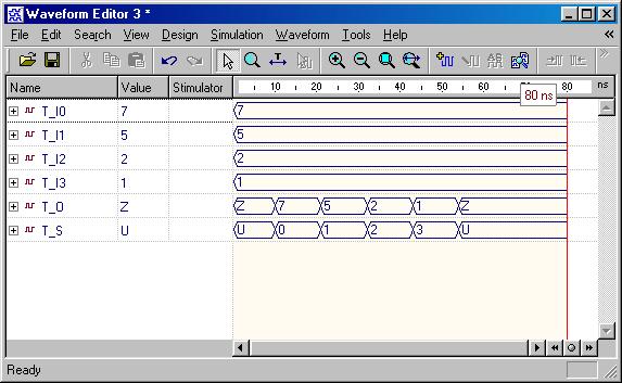
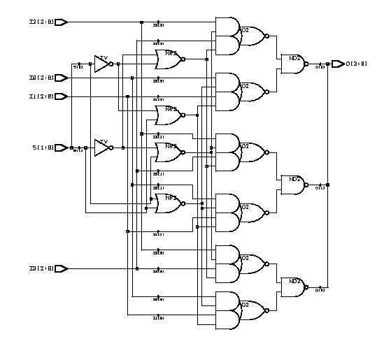
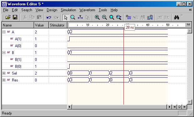
The following behavior style codes demonstrate the concurrent and sequential capabilities of VHDL. The concurrent statements are written within the body of an architecture. They include concurrent signal assignment, concurrent process and component instantiations (port map statement). Sequential statements are written within aprocess statement, function or procedure. Sequential statement include case statement, if-then-else statement and loop statement.
Latch & Flip-Flops
(ESD Chapter 2.3)
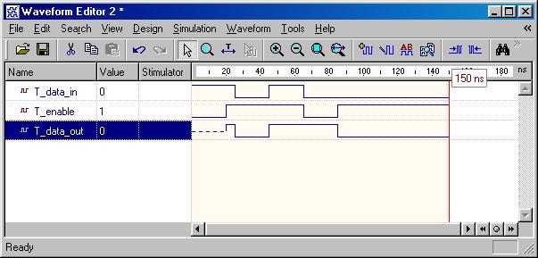
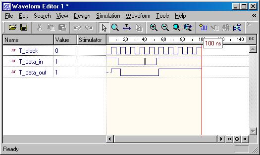
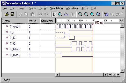
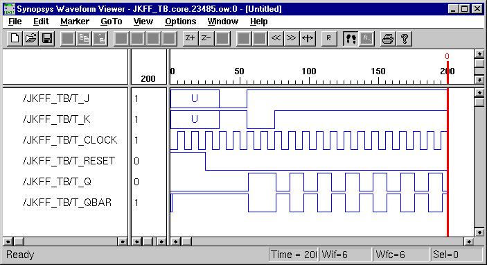
Besides from the circuit input and output signals, there are normally two other important signals, reset and clock, in the sequential circuit. The reset signal is eitheractive-high or active-low status and the circuit status transition can occur at either clock rising-edge or falling-edge. Flip-Flop is a basic component of the sequential circuits.
Typical Sequential Components
(ESD Chapter 2: Figure 2.6)
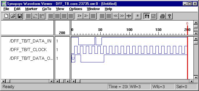
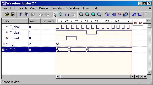
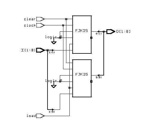
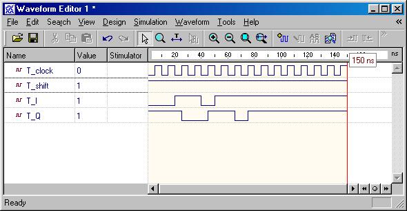
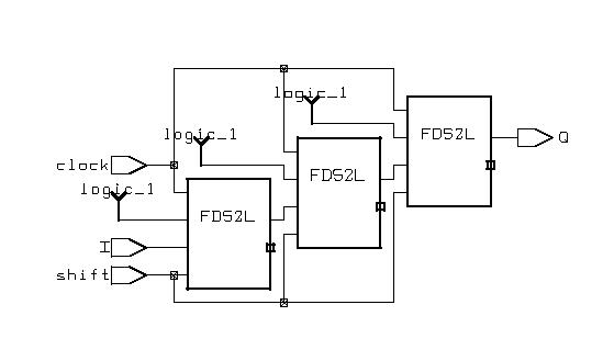
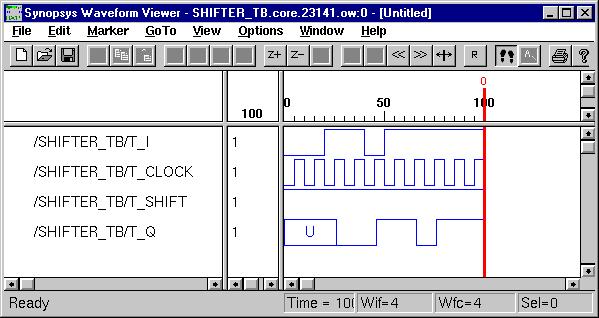
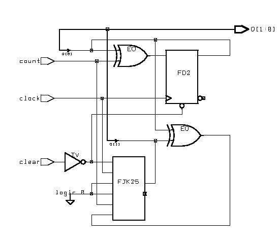
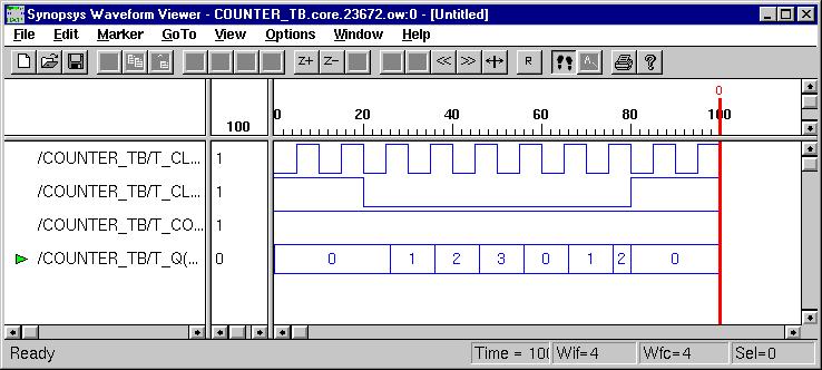
Typical sequential components consist of registers, shifters and counters. The concept of generics is often used to parameterize these components. Parameterized components make it possible to construct standardized libraries of shared models. In the behavioral description, the output transitions are generally set at the clock rising-edge. This is accomplished with the combination of the VHDL conditional statements (clock'event and clock='1'). During the testbench running, the expected output of the circuit is compared with the results of simulation to verify the circuit design.
Sequential Logic Design
(ESD Chapter 2: Figure 2.7)
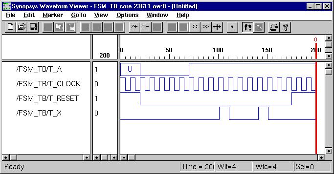
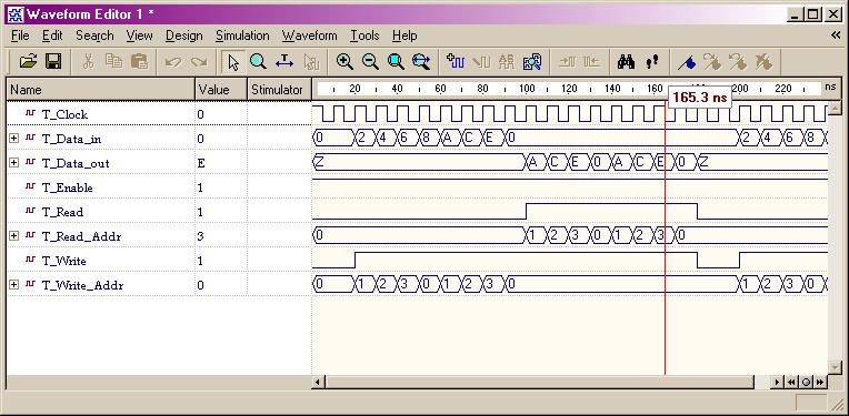
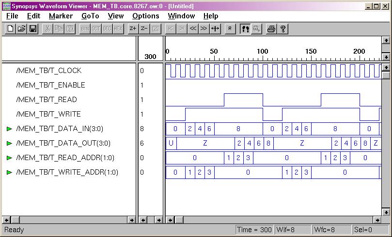
The most important description model presented here may be the Finite State Machine (FSM). A general model of a FSM consists of both the combinational Logic and sequential components such as state registers, which record the states of circuit and are updated synchronously on the rising edge of the clock signal. The output function computes the various outputs according to different states. Another type of sequential model is the memory module, which usually takes a long time to be synthesized due to the number of design cells.
- Memories (ESD Chapter 5)
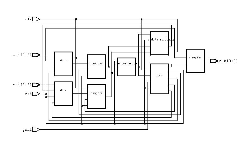
Following section illustrates the RTL (FSM+Datapath) method further using several design examples.
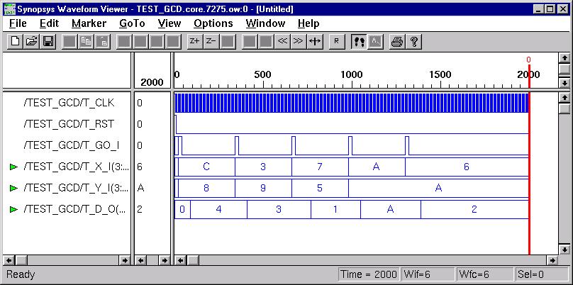
GCD Caculator
Behavior Code
RTL Code (FSM+D)
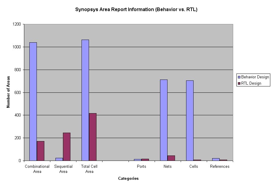
Comparison
Custom Single-Purpose Processor Design
(ESD Chapter 2, Chapter 4)
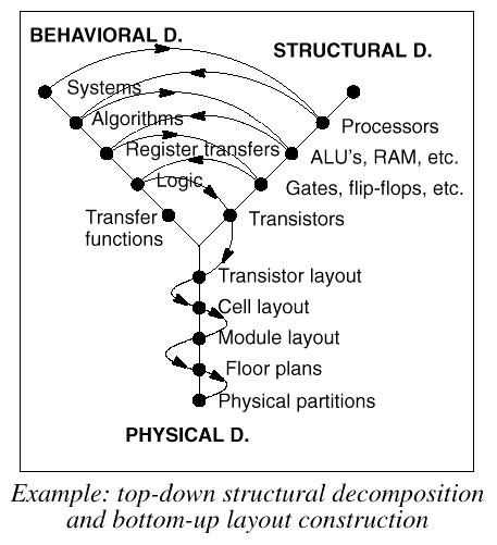
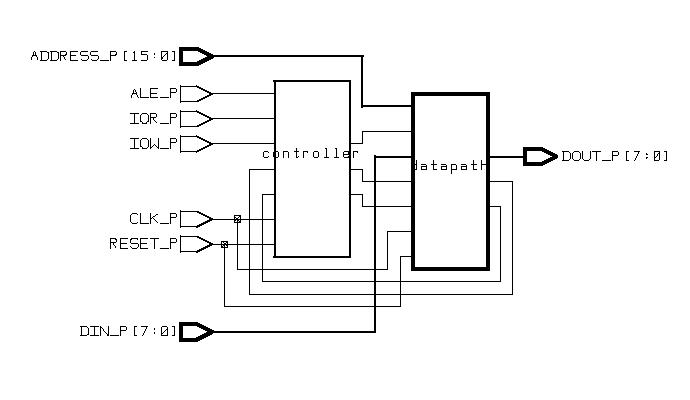
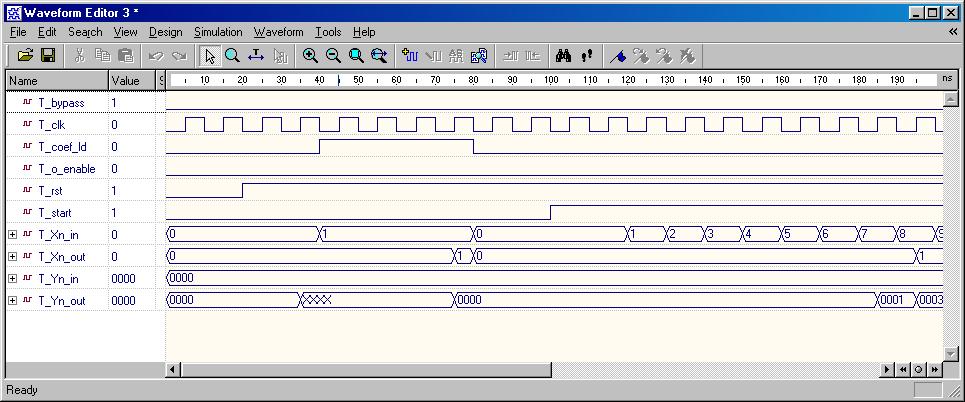
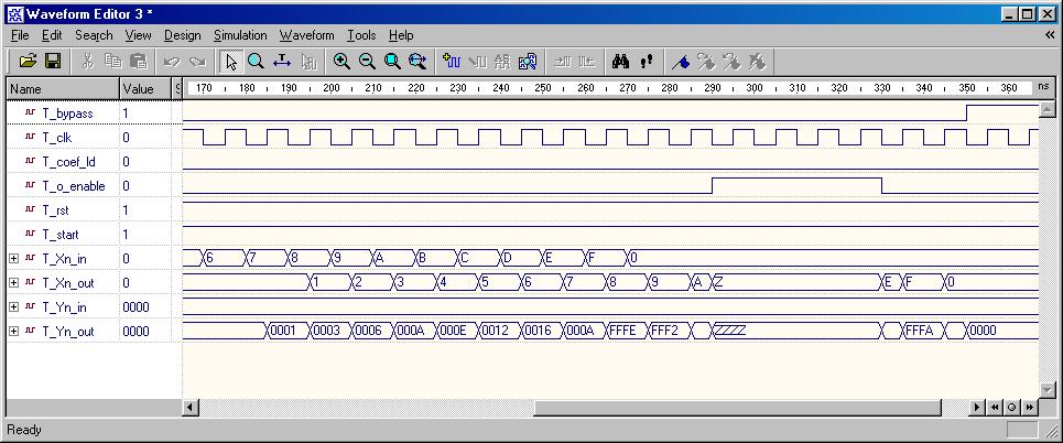
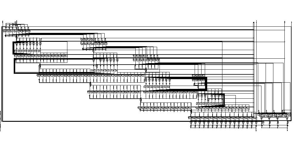
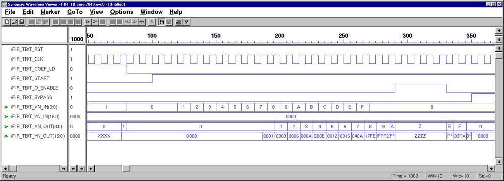
The first three examples illustrate the difference between RTL FSMD model (Finite State Machine with Datapath buildin) and RTL FSM + DataPath model. From view of RT level design, each digital design consists of a Control Unit (FSM) and a Datapath. The datapath consists of storage units such as registers and memories, and combinational units such as ALUs, adders, multipliers, shifters, and comparators. The datapath takes the operands from storage units, performs the computation in the combinatorial units, and returns the results to the storage units during each state. This process typically takes one or two clock cycles. Data-flow (looks more like an Algorithm) modeling is presented in the fourth example. The FIR digital filter algorithm is simulated and synthesized using VHDL. A comparison of the coding styles between the RTL modeling and Algorithm level modeling highlights the different techniques.
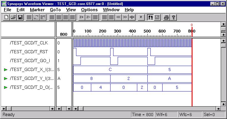
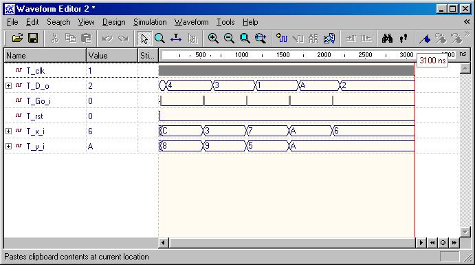
- GCD Calculator (ESD Chapter2: Figure 2.9-2.11)
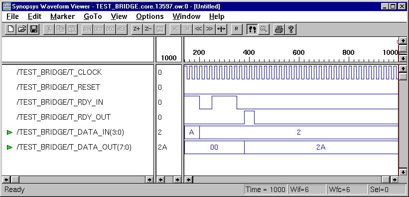
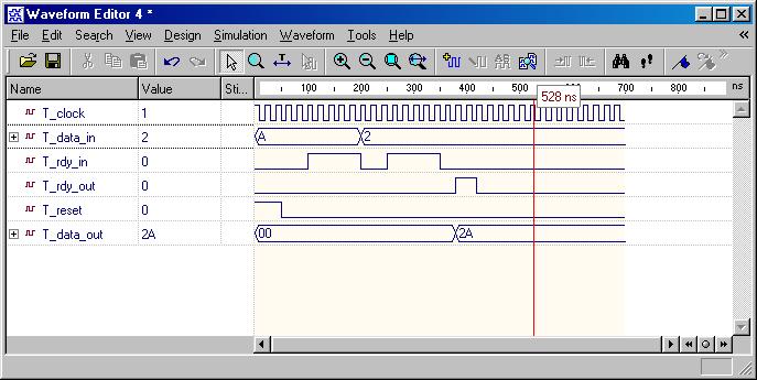
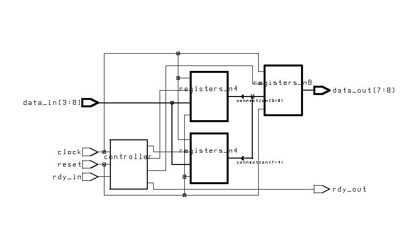
- Simple Bridge (ESD Chapter 2: Figure 2.13-2.14)
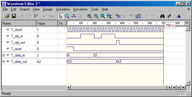
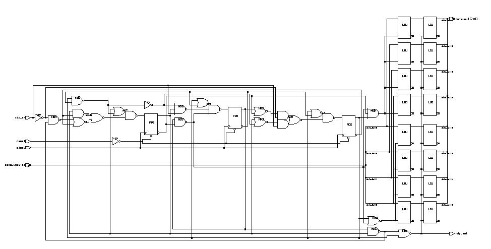
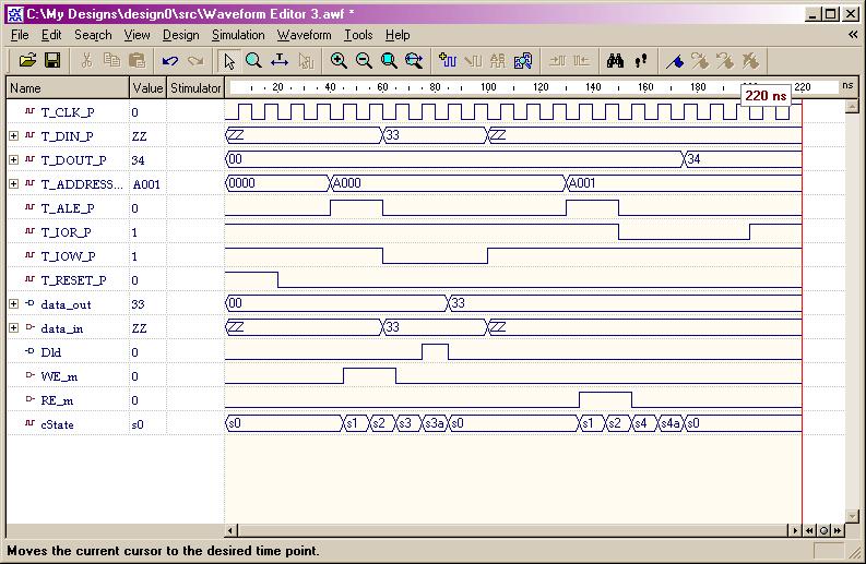
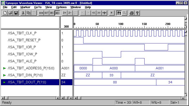
- ISA Bus Interface (ESD Chapter 4, Chapter 6)
- FIR Digital Filter (DSP Example)
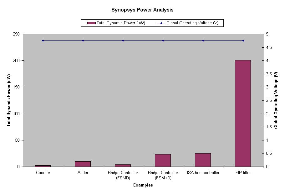
Synopsys tools can be used to perform Power Analysis for all the VHDL designs. Generally, the better design has smaller power consumption. On the other hand, improve the power always means sacrificing other design metrics such as performance, area size or NRE cost. Therefore, a designer need to balance these metrics to find the best implementation for the given application and constraints. Please check out the power analysis results of Adder, Counter, ISA controller, Bridge controller and FIR Filter. As we expected, FIR digital filter has the biggest power consumption because it has a more complex circuit doing DSP computation. Synopsys power analysis tutorial can be found here.
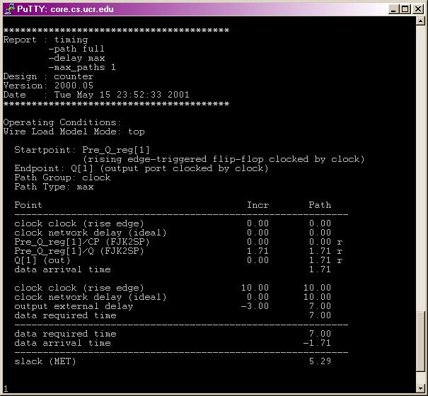
Another common way is to apply the timing constrains on the design during synthesis. then the timing report is checked to see if the slack, which is the required delay minus the actual delay, is MET or VIOLATED. If VIOLATED, we should go back to the VHDL code and re-write it to improve timing. The whole design will be compiled and tested again.
Counter
Behavior Code
Sythesis Script File
Timing Report
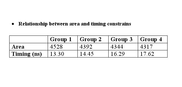
During Synopsys synthesis, ordinary combinational logic will go through several of what are known as mapping optimizations. In a normal optimization, the synthesis tool will optimize in relation to the set constrains. It is usual to talk about moving along a "banana curve" on the area and time axes. This means that the tougher the timing constrains, the larger the design will be, and vice versa. The results from two different synthesis constrains applied on the same design are shown below.
FIR filter
Sample Synthesis Script
Comparison Table
Banana Curve
General-Purpose Processor Design
(ESD Book Chapter 3, Figure 3.15)
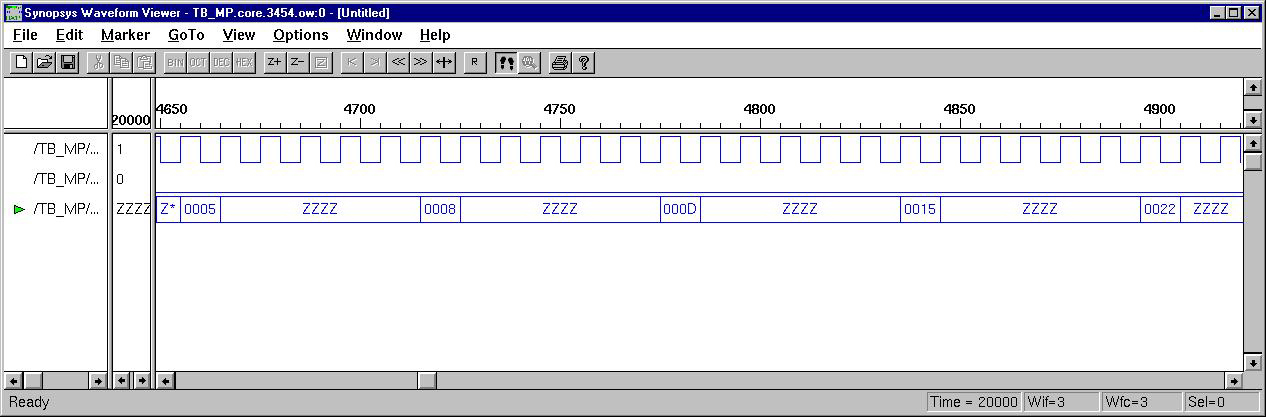
As indicated in the previous part, an Application Specific Integrated Circuit (ASIC) is specified with behavior descriptions which are presented in the form of particular algorithm or flowchart. A general purpose processor, on the other hand, is specified completely by its instruction set (IS). A sequence of instructions is required for the computation of a mathematical expression or any other similar computational task. To illustrate the whole procedure, a simple Pseudo-Microprocessor model is used which contains seven instructions (ESD book figure 3.7). The RT level design method from previous examples is used again to construct this microprocessor. The CPU will fetch, decode, and execute each instruction in order to get the final result. For test purposes, a short program (sequential instructions) is loaded into the memory. After execution, this program will obtain 10 Fabonacci Numbers, and store the results into specific memory address. The design was implemented using Active-HDL and Synopsys Design Compiler. (Please note that PC.vhd need a little modify to get correct synthesis result. Just a practice for the reader.)
Top Level Structural Code
microprocessor.vhd
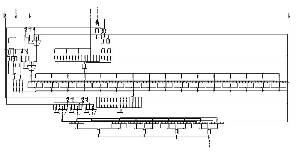
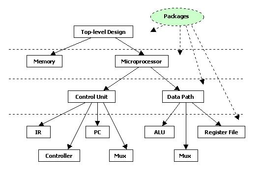
Design Hierarchy
cpuhierarchy.jpg
Test Bench of CPU Design
TB_mp.vhd
Control Unit
ctrl_unit.vhd
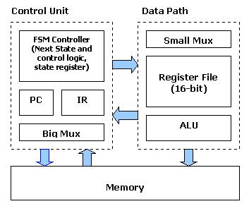
Block Diagram
cpublock.jpg
Data Path
datapath.vhd
controller.vhd PC.vhd
IR.vhd bigmux.vhd
Memory
memory.vhd
smallmux.vhd reg_file.vhd
alu.vhd obuf.vhd
Synopsys Sythesis Script Files
cpusyn.scr
syn_ctrl_unit.inc, syn_PC.inc, syn_IR.inc, syn_datapath.inc, syn_reg_file.inc
syn_alu.inc, syn_memory.inc
syn_controller.inc, syn_obuf.inc, syn_bigmux.inc, syn_smallmux.inc
Behavor Simulation
Script File
cpusim.scr
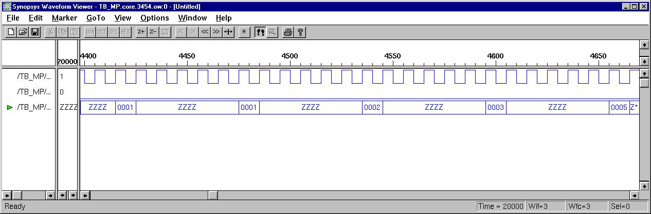
Simulation Waveform
cpusim1.jpg cpusim2.jpg
Gate-Level Simulation
Script File
cpugatesim.scr

















0 comments:
Post a Comment